- 您现在的位置:买卖IC网 > Sheet目录1998 > ICS84314AY-02LFT (IDT, Integrated Device Technology Inc)IC SYNTHESIZER 700MHZ 32-LQFP
700MHZ, CRYSTAL-TO-3.3V/2.5V LVPECL FREQUENCY
SYNTHESIZER w/FANOUT BUFFER
ICS84314-02
IDT / ICS 3.3V/2.5V LVPECL FREQUENCY SYNTHESIZER
1
ICS84314AY-02 REV. A MARCH 24, 2009
General Description
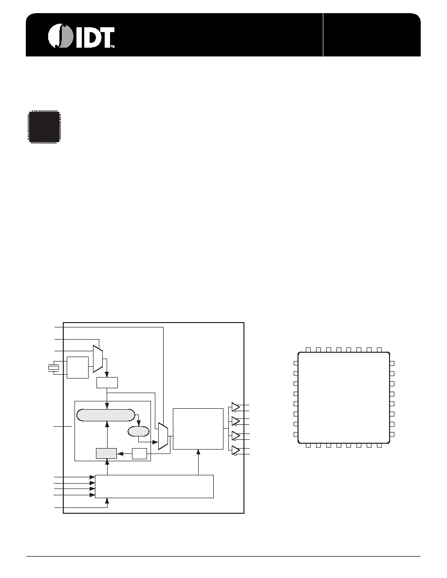
The ICS84314-02 is a general purpose quad output
frequency synthesizer and a member of the
HiPerClockS family of High Performance Clock
Solutions from IDT. When the device uses parallel
loading, the M bits are programmable and the output
divider is hard-wired for divide by 2 thus providing a frequency
range of 125MHz to 350MHz. In serial programming mode, the M
bits are programmable and the output divider can be set for either
divide by 1, 2, 4 or divide by 8, providing a frequency range of
31.25MHz to 700MHz. Additionally, the device supports spread
spectrum clocking (SSC) for minimizing Electromagnetic Interfer-
ence (EMI). The low cycle-cycle jitter and broad frequency range
of the ICS84314-02 make it an ideal clock generator for a variety
of demanding applications which require high performance.
Features
Fully integrated PLL
Four differential 3.3V or 2.5V LVPECL output pairs
Selectable crystal oscillator interface
or LVCMOS/LVTTL TEST_CLK input
Output frequency range: 31.25MHz to 700MHz
VCO range: 250MHz to 700MHz
Parallel interface for programming M dividers
Supports Spread Spectrum Clocking (SSC)
Down spread: -0.6%
Serial 3 wire interface
Cycle-to-cycle jitter: 45ps (maximum)
Output skew: 40ps (maximum)
Output duty cycle: 47% – 53%
Full 3.3V or mixed 3.3V core, 2.5V output operating supply
0°C to 70°C ambient operating temperature
Industrial temperature information available upon request
Available in both standard (RoHS 5) and lead-free (RoHS 6)
packages
HiPerClockS
ICS
OSC
VCO
PLL
Q0
nQ0
Q1
nQ1
Q2
nQ2
Q3
nQ3
Output Divider N
÷1
÷2 (Power-up Default)
÷4
÷8
CONFIGURATION
INTERFACE
LOGIC
÷ M
0
1
0
1
÷ 16
PHASE DETECTOR
VCO_SEL
XTAL_SEL
TEST_CLK
XTAL_IN
XTAL_OUT
MR
S_LOAD
S_DATA
S_CLOCK
nP_LOAD
M0:M8
÷2
PU
PD
9
10 11 12 13 14 15 16
32 31 30
29 28
27 26 25
1
2
3
4
5
6
7
8
24
23
22
21
20
19
18
17
M4
M5
M6
M7
M8
VEE
VCC
VCCO
TEST_CLK
XTAL_SEL
VCCA
S_LOAD
S_DATA
S_CLOCK
MR
VCCO
Q0
nQ0
Q1
nQ
1
Q2
nQ
2
Q3
nQ
3
M2
M1
M0
VCO_SEL
nP_LOAD
XTAL_OUT
XTAL_IN
M3
Block Diagram
Pin Assignment
ICS84314-02
32 Lead LQFP
Y Package
7mm x 7mm x 1.4mm package body
Top View
NOTE: Pullup (PU) and Pulldown (PD) refer to internal input resistors.
See Table 2, Pin Characteristics, for typical values.
发布紧急采购,3分钟左右您将得到回复。
相关PDF资料
ICS843156AKILF
IC CLK GENERATOR 32VFQFP
ICS843156AKLF
IC CLK GENERATOR 32VFQFP
ICS843202AYILF
IC SYNTHESIZER 680MHZ 32-LQFP
ICS843204AGILF
IC SYNTHESIZER LVPECL 48-TSSOP
ICS84320AY-01LN
IC SYNTHESIZER GP LVPECL 32-LQFP
ICS84320AYI-01LF
IC FREQ SYNTHESIZER 32TQFP
ICS843251AG-04LF
IC CLK GENERATOR LVPECL 8-TSSOP
ICS843251AGI-14LF
IC CLK GEN ETHERNET 25MHZ 8TSSOP
相关代理商/技术参数
ICS84314AY-02T
制造商:ICS 制造商全称:ICS 功能描述:700MHZ, CRYSTAL-TO-3.3V/2.5V LVPECL FREQUENCY SYNTHESIZER W/FANOUT BUFFER
ICS84314AYLF
功能描述:IC SYNTHESIZER 350MHZ 32-LQFP RoHS:是 类别:集成电路 (IC) >> 时钟/计时 - 时钟发生器,PLL,频率合成器 系列:HiPerClockS™ 标准包装:1,000 系列:- 类型:时钟/频率合成器,扇出分配 PLL:- 输入:- 输出:- 电路数:- 比率 - 输入:输出:- 差分 - 输入:输出:- 频率 - 最大:- 除法器/乘法器:- 电源电压:- 工作温度:- 安装类型:表面贴装 封装/外壳:56-VFQFN 裸露焊盘 供应商设备封装:56-VFQFP-EP(8x8) 包装:带卷 (TR) 其它名称:844S012AKI-01LFT
ICS84314AYLFT
功能描述:IC SYNTHESIZER 350MHZ 32-LQFP RoHS:是 类别:集成电路 (IC) >> 时钟/计时 - 时钟发生器,PLL,频率合成器 系列:HiPerClockS™ 标准包装:1,000 系列:- 类型:时钟/频率合成器,扇出分配 PLL:- 输入:- 输出:- 电路数:- 比率 - 输入:输出:- 差分 - 输入:输出:- 频率 - 最大:- 除法器/乘法器:- 电源电压:- 工作温度:- 安装类型:表面贴装 封装/外壳:56-VFQFN 裸露焊盘 供应商设备封装:56-VFQFP-EP(8x8) 包装:带卷 (TR) 其它名称:844S012AKI-01LFT
ICS84314AYT
制造商:ICS 制造商全称:ICS 功能描述:350MHZ, CRYSTAL-TO-3.3V/2.5V LVPECL FREQUENCY SYNTHESIZER W/FANOUT BUFFER
ICS843156AKILF
功能描述:IC CLK GENERATOR 32VFQFP RoHS:是 类别:集成电路 (IC) >> 时钟/计时 - 时钟发生器,PLL,频率合成器 系列:HiPerClockS™ 标准包装:1,000 系列:- 类型:时钟/频率合成器,扇出分配 PLL:- 输入:- 输出:- 电路数:- 比率 - 输入:输出:- 差分 - 输入:输出:- 频率 - 最大:- 除法器/乘法器:- 电源电压:- 工作温度:- 安装类型:表面贴装 封装/外壳:56-VFQFN 裸露焊盘 供应商设备封装:56-VFQFP-EP(8x8) 包装:带卷 (TR) 其它名称:844S012AKI-01LFT
ICS843156AKILFT
功能描述:IC CLK GENERATOR 32VFQFP RoHS:是 类别:集成电路 (IC) >> 时钟/计时 - 时钟发生器,PLL,频率合成器 系列:HiPerClockS™ 标准包装:1,000 系列:- 类型:时钟/频率合成器,扇出分配 PLL:- 输入:- 输出:- 电路数:- 比率 - 输入:输出:- 差分 - 输入:输出:- 频率 - 最大:- 除法器/乘法器:- 电源电压:- 工作温度:- 安装类型:表面贴装 封装/外壳:56-VFQFN 裸露焊盘 供应商设备封装:56-VFQFP-EP(8x8) 包装:带卷 (TR) 其它名称:844S012AKI-01LFT
ICS843156AKLF
功能描述:IC CLK GENERATOR 32VFQFP RoHS:是 类别:集成电路 (IC) >> 时钟/计时 - 时钟发生器,PLL,频率合成器 系列:HiPerClockS™ 标准包装:1,000 系列:- 类型:时钟/频率合成器,扇出分配 PLL:- 输入:- 输出:- 电路数:- 比率 - 输入:输出:- 差分 - 输入:输出:- 频率 - 最大:- 除法器/乘法器:- 电源电压:- 工作温度:- 安装类型:表面贴装 封装/外壳:56-VFQFN 裸露焊盘 供应商设备封装:56-VFQFP-EP(8x8) 包装:带卷 (TR) 其它名称:844S012AKI-01LFT
ICS843156AKLFT
功能描述:IC CLK GENERATOR 32VFQFP RoHS:是 类别:集成电路 (IC) >> 时钟/计时 - 时钟发生器,PLL,频率合成器 系列:HiPerClockS™ 标准包装:1,000 系列:- 类型:时钟/频率合成器,扇出分配 PLL:- 输入:- 输出:- 电路数:- 比率 - 输入:输出:- 差分 - 输入:输出:- 频率 - 最大:- 除法器/乘法器:- 电源电压:- 工作温度:- 安装类型:表面贴装 封装/外壳:56-VFQFN 裸露焊盘 供应商设备封装:56-VFQFP-EP(8x8) 包装:带卷 (TR) 其它名称:844S012AKI-01LFT